Researchers at Stanford University, in collaboration with the Belgian research center Imec, have developed a new manufacturing approach that enables the scalable production of semi-transparent and low-cost solar cells using tungsten instead of silicon.
Also known as transition metal dichalcogenide or TMD solar cells, these boast higher absorption coefficients and semiconductor properties compared to silicon.
An increasing demand for cleaner and greener energy has increased wind and solar installations worldwide. While wind turbines are getting bigger by the day and are moving offshore, solar panels offer the flexibility of installations even in crowded spaces like cities.
Interesting Engineering has previously reported how solar panels are adorning balconies in Europe and offering users the choice to reduce their dependence on fossil fuels while still being connected to the grid.
For years, transparent solar panels have been touted as the next windows, allowing light to enter buildings and serving as power generation sources. A major hurdle in this dream has been the opacity of solar panels, which could be solved with TMD solar cells.
What are TMD solar cells?
TMD solar cells promise to be highly efficient since they have higher absorption coefficients. However, TMD is two-dimensional and offers two additional advantages. First, the material is highly flexible and can be used on various surfaces.
The other is that it can be used to make semi-transparent solar cells, which can be used in applications such as solar windows. Together, the TMD solar cells can revolutionize the use of solar energy in aerospace, wearables, and construction industries, where a lightweight and semi-transparent solar cell could be effective.
However, the production process of TMD solar cells could be more conducive to large-scale applications.
Mass production-friendly technique
Researchers at Stanford and Imec in Belgium collaborated to develop a new TMD-production technique that can produce wafer-scale tungsten diselenide (WSe2) films with a layered van der Waals structure, a preprint paper said.
This technique boosted the charge carrier lifetime of the material to 144 ns, which is 14 times better than any TMD film produced earlier, the researchers added.
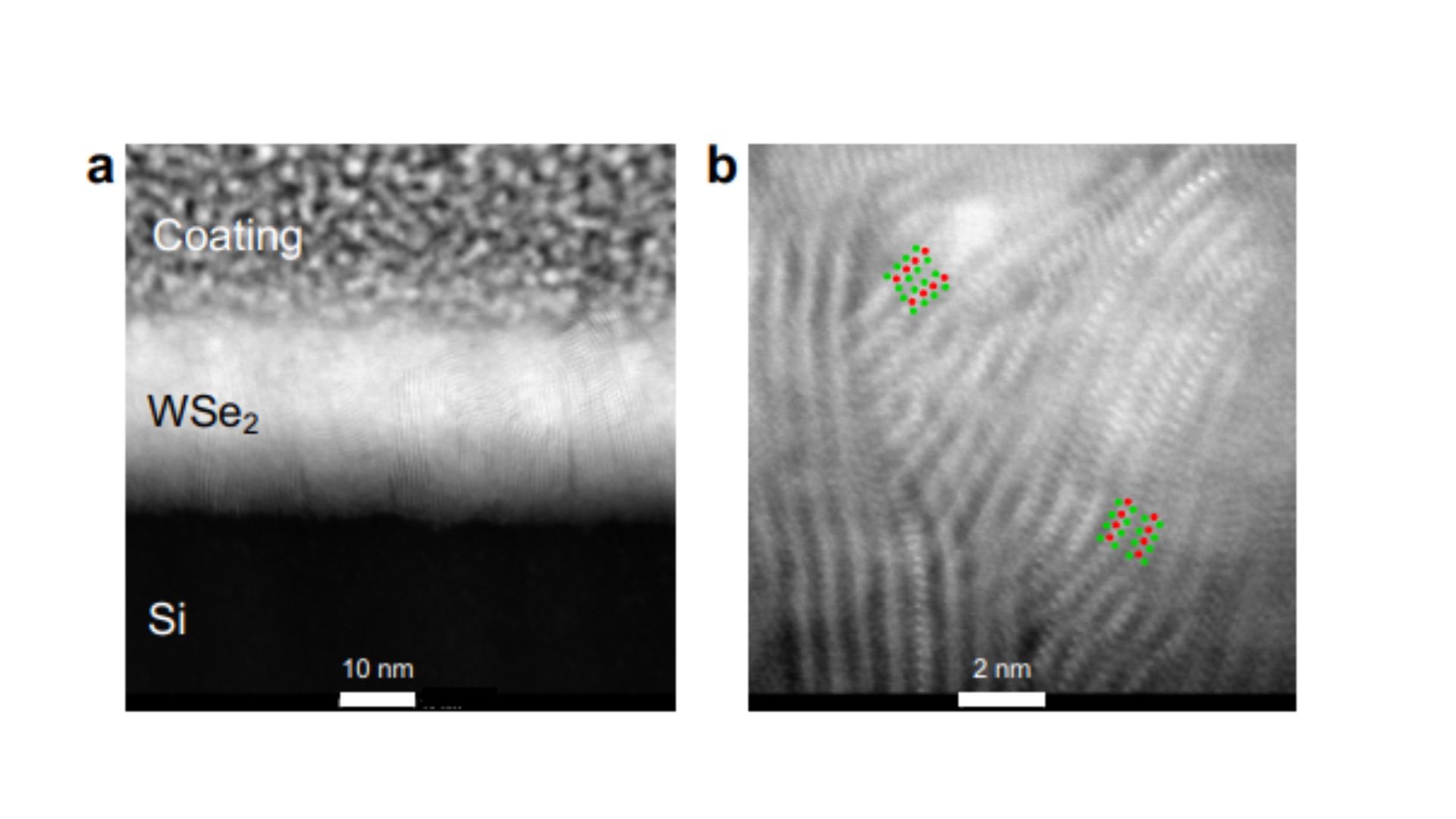
Transmission electron microscopy (TEM) of H2Se-selenized films. a, Cross-sectional view of selenized films on a silicon substrate with a metallic coating. b) A higher magnification image showing the varied orientation of lamella. Image credit: Stanford University/ arxiv.
Their collaboration resulted in a sputtered multilayer WSe2 film no thicker than 30 nm placed on a 150 mm wafer. The researchers used two selenization approaches: solid source selenium (SS-Se) or hydrogen selenide (H2Se) precursor.
The solid-state selenium requires a higher temperature of 1650 degree Fahrenheit (900 degree Celsius), while H2Se selenization can occur at 1200 degree Fahrenheit (650 degree Celsius). Irrespective of the process used, the WSe2 film generated has an energy bandgap of 1.2 to 1.3eV, making it ideal for use in a solar cell.
According to the researchers, by improving doping and contacts, the solar cell can reach an energy conversion efficiency of 22.3 percent. This is comparable to commercially available solar cells and paves the way for the widespread use of flexible solar cells in various applications.
The researchers added that the WSe2 solar cells’ higher carrier lifetimes could deliver a power rating of 64 W per gram in a packaged cell or up to 3W per gram in a solar module. The production process is not only simple but also low-cost, promising a new future for photovoltaics and nanoelectronics alike.
RECOMMENDED ARTICLES
The research findings were published in the preprint server, arxiv.
0COMMENT
NEWSLETTER
The Blueprint Daily
Stay up-to-date on engineering, tech, space, and science news with The Blueprint.
Ameya Paleja Ameya is a science writer based in Hyderabad, India. A Molecular Biologist at heart, he traded the micropipette to write about science during the pandemic and does not want to go back. He likes to write about genetics, microbes, technology, and public policy.


0